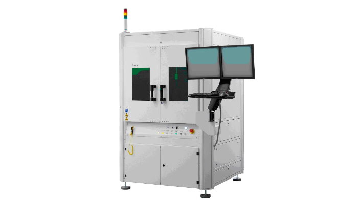
ficonTEC Wafer-level photonic device test
1
2
機能・特性
- Automated I/O port referencing to sub-µm accuracy
- Vertical and edge alignment to I/O ports in max. 4s
- Low-loss I/O port coupling with <0.4 dB repeatability
- Superior test data acquisition over manual approach
- Wafer fabs receive PIC yield data across entire wafer
製品情報
-
MANUFACTURER
ficonTEC -
MANUFACTURING PROCESS
Optoelectronic communication -
SERIES PRODUCTS
WT800/WT1200/WT1600/WT2000 -
General tasks & applications
Automated test-&-qualify for passive/active devices - Proof-of-concept and low-complexity volume e/o test
- MPW-capable due to adaptable probe-wafer layout
- Off-wafer device capable with suitable carrier formats
- Adaptable to high-complexity co-packaged applications
- For communications, sensors/lidar/IoT and 3D scanning